
Traditional Buck Converter Operation Mode:
Continuous current mode: Buck converters operate in continuous mode if the current through the inductor never falls to zero during the commutation cycle. In this mode, the operating principle is described by the plots in figure
Discontinuous current mode: In some cases, the amount of energy required by the load is too small. In this case, the current through the inductor falls to zero during part of the period. The only difference in the principle described above is that the inductor is completely discharged at the end of the commutation cycle (see figure 5). This has, however, some effect on the previous equations.
Efficiency
There are two main phenomenon impacting the efficiency: conduction losses and switching losses.
Conduction losses happen when current is flowing through the components and thus depend on the load. They are caused by Joule effect in the resistance when the transistor or MOSFET switch is conducting, the inductor winding resistance, and the capacitor equivalent series resistance. Losses are proportional to the square of the current in this case. Conduction losses are also generated by the diode forward voltage drop (usually 0.7 V or 0.4 V for schottky diode), and are proportional to the current in this case.
Switching losses happen in the transistor and diode when the voltage and the current overlap during the transitions between closed and open states. A schottky diode can be used to minimize the switching losses caused by the reverse recovery of a regular PN diode. The switching losses are proportional to the switching frequency.
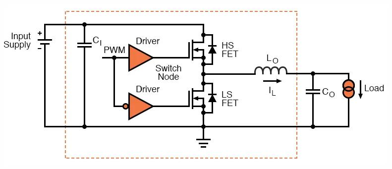
In a complete real-world buck converter, there is also a command circuit to regulate the output voltage or the inductor current. This circuit and the MOSFET gate controller have a power consumption, impacting the overall efficiency of the converter.
Output voltage ripple is the name given to the phenomenon where the output voltage rises during the On-state and falls during the Off-state. Several factors contribute to this including, but not limited to, switching frequency, output capacitance, inductor, load and any current limiting features of the control circuitry. At the most basic level the output voltage will rise and fall as a result of the output capacitor charging and discharging:

We can best approximate output ripple voltage by shifting the output current versus time waveform (continuous mode) down so that the average output current is along the time axis. When we do this, we see the AC current waveform flowing into and out of the output capacitor (sawtooth waveform). We note that Vc-min (where Vc is the capacitor voltage) occurs at ton/2 (just after capacitor has discharged) and Vc-max at toff/2. By integrating Idt (= dQ ; as I = dQ/dt, C = Q/V so dV = dQ/C) under the output current waveform through writing output ripple voltage as dV = Idt/C we integrate the area above the axis to get the peak-to-peak ripple voltage as: ΔV = ΔI T/8C (where ΔI is the peak-to-peak ripple current and T is the time period of ripple. A full explanation is given there.) We note from basic AC circuit theory that our ripple voltage should be roughly sinusoidal: capacitor impedance times ripple current peak-to-peak value, or ΔV = ΔI / (2ωC) where ω = 2πf, f is the ripple frequency, and f = 1/T, T the ripple period. This gives: ΔV = ΔI T/2πC), and we compare to this value to confirm the above in that we have a factor of 8 vs a factor of ~ 6.3 from basic AC circuit theory for a sinusoid. This gives confidence in our assessment here of ripple voltage. The paragraph directly below pertains that directly above and may be incorrect. Use the equations in this paragraph. Once again, please see talk tab for more: pertaining output ripple voltage and AoE (Art of Electronics 3rd edition).
During the Off-state, the current in this equation is the load current. In the On-state the current is the difference between the switch current (or source current) and the load current. The duration of time (dT) is defined by the duty cycle and by the switching frequency.
For the on-state:

For the off-state:

Qualitatively, as the output capacitance or switching frequency increase, the magnitude of the ripple decreases. Output voltage ripple is typically a design specification for the power supply and is selected based on several factors. Capacitor selection is normally determined based on cost, physical size and non-idealities of various capacitor types. Switching frequency selection is typically determined based on efficiency requirements, which tends to decrease at higher operating frequencies, as described below in Effects of non-ideality on the efficiency. Higher switching frequency can also raise EMI concerns.
Output voltage ripple is one of the disadvantages of a switching power supply, and can also be a measure of its quality.
- Reference wiki
